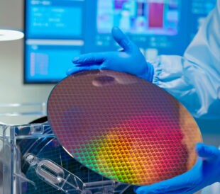
Ultra-high-purity gases are essential to semiconductor manufacturing, where even trace contaminants can compromise yield, reliability, and productivity. Modern wafer fabrication relies on a clean, stable gas infrastructure to support deposition, etching, lithography, and thermal treatments. As device geometries shrink and process windows tighten, the industry’s tolerance for contamination continues to approach zero.
A key analytical technology enabling this progress is atmospheric-pressure ionization mass spectrometry (APIMS). This technique measures impurities in bulk gases at extremely low concentrations—down to the parts-per-trillion (ppt) range—providing near-real-time insight into gas purity and upstream system performance. The following article summarizes how APIMS works, why it is uniquely suited for semiconductor gas monitoring, and how ongoing innovations continue to lower detection limits.
What Is Atmospheric-Pressure Ionization Mass Spectrometry?
APIMS differs from traditional mass spectrometry because it ionizes gas molecules at atmospheric pressure rather than under high vacuum. Instead of requiring pressure conditioning or complex sample preparation, ultra high purity (UHP) electronic gas analyzers accept gas directly from the purified supply line. This simplifies operation and eliminates many contamination challenges common to conventional electron-impact techniques.
Ionization occurs through a high-voltage corona discharge in which thousands of volts generate a dense plasma of ionized gas molecules. Because impurities in semiconductor gases exist at ppt levels, there are far fewer impurity molecules than bulk-gas molecules in the ionization region. APIMS overcomes this through two key mechanisms:
- Charge Transfer Ionization
- Impurities often have lower ionization potentials than the bulk gas. When ionized bulk-gas molecules collide with impurity molecules, charge transfers preferentially to the impurity. This effect amplifies impurity signals, bypassing the background noise challenges that limit traditional approaches.
- Proton Transfer Ionization
- In hydrogen, ionized H₃⁺ clusters can donate a proton to impurities with high proton affinity—such as water, CO, CO₂, and methane. These impurity species become easily detectable, further improving sensitivity.
Together, these processes allow APIMS to detect contaminants at levels no other analytical platform can reliably observe.
Why Semiconductor Manufacturing Requires PPT Detection
Semiconductor gases—including helium, nitrogen, argon, and hydrogen—must remain pure throughout distribution networks, storage vessels, and cleanroom delivery. Trace methane, oxygen, moisture, and other contaminants disrupt oxidation rates, etch uniformity, or downstream chemical reactions.
APIMS’ ability to monitor gases at ppt concentrations provides several advantages:
- Immediate detection of system-level issues such as purifier degradation, leaks, outgassing, or inconsistent vessel vaporization.
- Clear differentiation between seemingly pure gases—e.g., identifying when “100 ppt” methane in argon is actually unacceptable compared to a <10 ppt optimal baseline.
- Trend visibility for cyclic variations driven by cryogenic vessel behavior or process load changes.
- Compatibility with multiple bulk gas types, except pure oxygen, whose ionization potential limits charge-transfer behavior.
These insights allow engineers to proactively protect valuable wafers, reducing scrap, downtime, and yield excursions.
Demonstrated Sensitivity and Linearity
In real-world cases, APIMS routinely measures:
- Methane in argon at 40–100 ppt, distinguishing between process variation and contamination issues.
- Methane in argon below 10 ppt once a system fault is corrected.
- Oxygen in nitrogen with linearity extending from ppb calibration down to ppt, enabled by a background of only ~6 ppt.
- Standard deviation performance better than 1 ppt, confirming measurement stability.
These measurements illustrate why the technique is considered the most sensitive analytical approach available for ultra-high-purity gases.
Technology Enhancements for Future Detection Limits
Ongoing development focuses on further reducing detection limits. One area of study involves optimizing the declustering region, where pressure and geometry influence ion-cluster formation. Experimental redesigns of internal components have shown up to 10× improvements in signal sensitivity for certain impurities.
Additional research includes:
- Improved hydrocarbon monitoring, enabling ppt-level measurements of species such as ethane without interference from methane.
- Detection of noble gases such as krypton and xenon, which support non-semiconductor applications including safety monitoring in nuclear power generation.
These advancements expand APIMS’ relevance as purity requirements intensify.
Modern systems support multi-stream, multi-component analysis, enabling rapid cycling across multiple gas lines. Continuous 24/7 monitoring ensures that even transient contamination events are captured. In semiconductor environments where wafer lots can be valued in the millions, continuous surveillance is no longer optional—it is central to process integrity.
Conclusion
As semiconductor manufacturing advances toward ever-smaller geometries and increasingly stringent purity requirements, parts-per-trillion gas analysis has become essential for protecting wafer integrity and maintaining stable production environments.
Atmospheric-pressure ionization mass spectrometry delivers the sensitivity, specificity, and real-time insight needed to detect contaminants long before they affect process performance. By combining atmospheric-pressure ionization with charge-transfer and proton-transfer mechanisms, APIMS empowers fabs to monitor impurities with exceptional precision, troubleshoot system irregularities, and proactively safeguard yield. With ongoing innovation pushing detection limits even lower, this technology remains a cornerstone of modern gas-quality assurance and a critical enabler of next-generation semiconductor manufacturing.
Additional Resources
- Learn more about ultra-high purity electronic gas analyzers in the semiconductor industry
- Webinar: Ultra-pure gas for higher yield: Gas analysis for semiconductor manufacturing
- Infographic: 5 reasons to use ultra high purity gas analyzers in the semiconductor industry
- Infographic: Visualizing parts per trillion – The hunt for semiconductor process gas impurities
- Ultra high purity (UHP) electronic gas analyzers
FAQs
- Why do semiconductor fabs require parts-per-trillion gas analysis?
- Because nanometer-scale device features are extremely sensitive to chemical variability, ppt-level contaminants can lead to defects, yield loss, or process drift. APIMS provides the necessary sensitivity.
- How does APIMS differ from traditional mass spectrometry?
- It ionizes gases at atmospheric pressure without vacuum-related background effects, enabling superior trace detection and simplified sample handling.
- Can APIMS measure multiple impurities in multiple gases?
- Yes. Modern systems monitor several gas lines and measure impurities such as moisture, methane, oxygen, CO, CO₂, and hydrocarbons at ppt levels.
- What limits the ability to detect impurities in oxygen?
- Oxygen has a low ionization potential, reducing the ionization-potential difference required for efficient charge transfer.
- How does APIMS improve contamination troubleshooting?
- Trend data reveals leak events, purifier failures, abnormal vaporization patterns, or system faults that affect purity.
How Gas Purity Protects Yield, Quality, and Uptime in Semiconductor Fabs
As the global appetite for smarter, faster, and more powerfu... Daniel Merriman
Read More
The Silent Revolution: How Semiconductor Advancements Are Reshaping Our World
In an era where technology dictates the speed of progress, s... Whitney Hatcher
Read More
Invisible Threats: The Semiconductor Industry’s Battle Against Contamination
The semiconductor industry is facing a paradox. As technolog... Whitney Hatcher
Read More
Why Use FTIR to Measure Epitaxial Layers in Semiconductors?
In the semiconductor industry, accurate and efficient measur...
Read More
Leave a Reply