Challenges of non-conductive sample imaging Electron microsc... Alice Scarpellini
Read More Analyzing Non-Conductive Material with Low-Vacuum SEM Imaging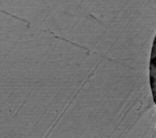
Spectroscopy, spectrometry, and materials science stories and solutions about advancing research and improving product development
Challenges of non-conductive sample imaging Electron microsc... Alice Scarpellini
Read More Analyzing Non-Conductive Material with Low-Vacuum SEM Imaging
In process analytical technology (PAT), few innovations have... Janam Pandya
Read More Modular Multiplex Raman vs. Traditional Multiplexing: A Smarter Approach to Process Monitoring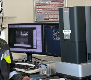
By upgrading their scanning electron microscope (SEM), the V...
Read More Phenom Desktop SEM for Industrial Quality Control: How Vesuvius Foseco Improved Aluminum Cleanliness Testing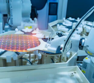
Ultra-high-purity gases are essential to semiconductor manuf... Daniel Merriman
Read More How Parts-Per-Trillion Gas Analysis Protects Semiconductor Wafer Production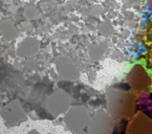
Microstructural analysis of advanced materials There is a ri...
Read More Live SEM EDS Enhances the Microstructure Analysis of Steel
Plastic beads—an iconic part of Mardi Gras celebrations—... Marlene Gasdia-Cochrane, Editor
Read More Can Plastic Beads Cause Mardi Gras Misfortune? Investigating Toxic Metals and Materials