One of the great things about working within the semiconductor industry is seeing the impact of semiconductors and new applications changing the way the world works, plays, learns and connects. Logic and memory with new, more complex structures continue to evolve to deliver smaller, denser and more powerful chips. Power devices are evolving to support higher voltages, faster switching and greater power efficiency. Display manufacturers are improving existing technology and developing new technology to take displays to the next level.
While many of these semiconductor devices seem simple in concept, the reality is that significant manufacturing challenges are still present. For logic and memory manufacturers, the challenges may be associated with fabricating structures that are increasingly complex and 3-dimensional. For power and display manufacturers, challenges may be found in new compound materials impacted by unseen physical defects.
To address these challenges, there is a need to see what is going on inside the device to tune processes in real time and increase product reliability and yields. This is where 3D semiconductor reconstruction modeling can be a great asset for revealing defects and analyzing devices that other methodologies such as CD-SAX and OCD, can’t see.
What is 3D semiconductor reconstruction and how is it used?
For manufacturers, 3D semiconductor reconstruction provides a 3-dimensional view of devices that allow the user to make virtual slices in any direction. This capability can be incredibly valuable in efforts to identify defects and measure CDs (critical dimensions).
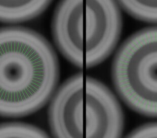
For example, 3D reconstruction lets manufacturers view 3D NAND memory etch profiles from the top to the bottom of the device as shown in the image below. This allows users to view tungsten voids and measure channel holes.

3D reconstruction provides top-down view of a 3D NAND memory device.
Another example where 3D semiconductor reconstruction can be a valuable tool is for visualizing surface roughness within a device. This is important as the surface roughness of a silicon wafer is one of the most important issues that degrade characteristics of semiconductor devices. From research conducted on MOSFETs, it’s been found that roughness with a low spatial wavelength affects electron mobility and gate insulating film reliability.

3D reconstruction showing surface roughness within a 3D NAND memory device.
Why FIB-SEM is key for 3D reconstruction in semiconductor devices
Constructing the 3D model is accomplished using a FIB-SEM such as a Thermo Scientific Helios 5 DualBeam for deprocessing and imaging the device and Thermo Scientific Avizo Software for visualization and analysis.
Where the most difficult challenges involve device structure (shape and layout) complexity, new materials, and the statistical limits of controlling stochastic processes for dimensional, compositional, surface, and interfacial measurements, 3D semiconductor reconstruction enables CD metrology on crazy 3D structures, and insight into understanding the structure-performance relationship of semiconductor devices.
For more information on this topic, please watch our on-demand SPARK webinar, Visualizing, analyzing and understanding semiconductor devices with 3D reconstruction.
Speak to one of our experts to learn how 3D semiconductor reconstruction modeling can help you address industry challenges.

Enhancing High-Volume DRAM Manufacturing with Automated TEM Metrology and Characterization
Dynamic random-access memory (DRAM) plays a crucial role in ... Dr. Zhenxin Zhong
Read More
Faster time to data in the fab with multi-ion species plasma FIB
This quarter, I am excited to share the news about a newly r...
Read MoreHigh-Quality TEM Lamella Preparation: Critical Factors and Best Practices
Introduction: The quality of transmission electron microscop... Abhi Barve
Read More
Removing Large Volumes of Material Fast with FIB-SEMs
Focused ion beam scanning electron microscopes (FIB-SEMs) ar...
Read More
Leave a Reply