Focused ion beam scanning electron microscopes (FIB-SEMs) are essential tools for preparing high-quality semiconductor samples for failure analysis and metrology. As semiconductors become more complex with 3D structures, packaged dies, novel materials, and higher circuit density, obtaining statistically relevant data with sub-nanometer accuracy is crucial for identifying defects and out-of-tolerance process steps.
Why is High-Quality Sample Preparation Critical for Semiconductor Analysis?
A high-quality sample devoid of damage and artifacts is required for various analytical tasks:
- Removing large volumes of material to locate nanometer-scale defects in large areas
- Removing small volumes of materials for site-specific analysis
- Preparing lamellae for transmission electron microscopy (TEM) analysis
Each of these applications presents unique challenges that can affect sample quality. This article focuses on high-speed, large-volume material removal and the characteristics needed in FIB-SEM systems to address these challenges.
What Challenges Arise When Removing Large Volumes of Material?
When performing large-volume material removal across semiconductor samples, three primary challenges emerge:
- Curtaining effects
- Sample damage
- Handling dissimilar materials
The correct FIB-SEM system can help mitigate these challenges and deliver high-quality samples for analysis.
How Do Curtaining Effects Impact Large-Volume Material Removal?
Curtaining occurs when milling with variable milling rates through samples that contain different materials. This interaction creates variations in topography that appear as scratches or striations on the milled face, potentially making detailed analysis difficult or impossible.
While curtaining can affect both small-volume and large-volume sample preparation, it propagates more rapidly with dissimilar materials and large cross-sections. To address this issue, look for instruments that support capabilities such as rocking polish.
What is Spin Mill and How Does it Help?
For uniform large-area planar milling, the spin mill technique is valuable. This process removes a thin layer from the sample surface at a nearly glancing angle while periodically rotating the stage to pre-defined milling sites. This efficiently removes material over a large planar area, providing a smooth surface for imaging, nanoprobing, or additional cross-sectioning work.
Both the Thermo Scientific Helios 5 PFIB-SEM and the Helios 5 Laser PFIB-SEM offer cross-sectioning and spin mill capabilities for large-volume material removal.
How Do Different Laser Types Affect Sample Quality?
When quickly removing large volumes of material over large areas, lasers offer unparalleled speed. While a plasma FIB (PFIB) enables material removal at approximately 10^6 μm³/hr, a laser can remove approximately 10 mm³/hr. However, not all lasers provide the same milling characteristics.
“Nanosecond” lasers can effectively remove material by ablation but may cause unwanted damage to surrounding areas. Microcracking can form in a large heat-affected zone due to thermal stresses, shock waves, and material melting and cooling.

Randolph, Steven & Filevich, Jorge & Botman, Aurelien et al. (2018). In situ femtosecond pulse laser ablation for large volume 3D analysis in scanning electron microscope systems. Journal of Vacuum Science & Technology B. 36. 06JB01. 10.1116/1.5047806.
Why Are Femtosecond Lasers Preferred?
Femtosecond (fs) lasers propagate energy in short pulses with greater instantaneous intensity. This quickly accelerates local ablation, preventing thermal energy transfer to surrounding material. Most of the absorbed energy gasifies the solid phase into plasma, minimizing thermal damage.
For optimal results, solutions that utilize an integrated femtosecond laser in a single chamber, such as the Thermo Scientific Helios 5 Laser PFIB-SEM, are recommended. This integration eliminates navigation misalignments and potential sample contamination that can occur with two-chamber systems or ex situ lasers.
What Challenges Arise When Preparing Samples with Dissimilar Materials?
Preparing samples with multiple types of stacked material is increasingly common, especially in 2.5D and 3D packages. These structures contain several hierarchal packaging levels with single or multiple dies, resulting in packages containing disparate materials, some soft and some hard like silicon carbide (SiC).
Stacked materials with different sputter rates can cause extreme curtaining and introduce unwanted thermal behaviors, potentially damaging the sample and hindering proper analysis.
How Do Ion Species and Beam Angle Affect Material Removal?
Two factors significantly impact the ability to remove large volumes of material and produce high-quality samples with dissimilar materials:
- Ion species
- Angle of incidence of the beam to the sample
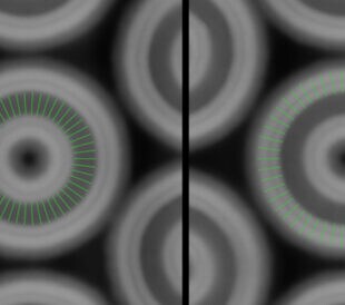
Different ion species mill more uniformly for different substrate types:
- Xenon (Xe) and argon (Ar) are non-interactive ion species ideal for cross-sectioning
- Oxygen (O) interacts both chemically and physically during milling, making it extremely effective for hard materials like silicon carbide (SiC), diamond, and other carbon-containing materials
 and argon-prepared (58 s at 3.7 μA) silicon samples.")
For samples containing multiple material types, the flexibility to switch between ion beam species in minutes is essential. The Thermo Scientific Helios 5 Hydra DualBeam offers this capability, making it invaluable for preparing and analyzing complex samples.
Comparison of FIB-SEM Technologies for Large-Volume Material Removal
| Technology | Material Removal Rate | Best Applications | Key Advantages |
| Plasma FIB | ~10^6 μm³/hr | Large-area cross-sectioning, spin mill | Balanced speed and precision |
| Laser PFIB | ~10 mm³/hr | Very large volume removal | Fastest material removal, integrated workflow |
| Multi-Ion Hydra | Varies by ion species | Samples with dissimilar materials | Flexibility to optimize for different materials |
Summary
Modern semiconductor sample preparation requires solutions for a wide variety of applications. When performing large-volume material removal, challenges such as curtaining, sample damage, and handling dissimilar materials can be mitigated with the appropriate FIB-SEM technology:
- Curtaining effects can be addressed with techniques like rocking polish and spin mill
- Femtosecond lasers minimize thermal damage when removing large volumes of material
- Different ion species (Xe, Ar, O) provide optimal milling for different material types
- Integrated systems eliminate navigation misalignments and sample contamination
The Thermo Scientific Helios 5 DualBeam family, including the PFIB, Laser PFIB, and Hydra systems, offers solutions tailored to these challenges, enabling high-quality sample preparation for advanced semiconductor analysis.
Enhancing High-Volume DRAM Manufacturing with Automated TEM Metrology and Characterization
Dynamic random-access memory (DRAM) plays a crucial role in ... Dr. Zhenxin Zhong
Read More
Faster time to data in the fab with multi-ion species plasma FIB
This quarter, I am excited to share the news about a newly r...
Read MoreHigh-Quality TEM Lamella Preparation: Critical Factors and Best Practices
Introduction: The quality of transmission electron microscop... Abhi Barve
Read More
Transmission Electron Microscopy in Semiconductors: Generating Ground Truth Insights
What is the current state of TEM in semiconductor analysis? ... Dominique Delille
Read More
Leave a Reply