What is the current state of TEM in semiconductor analysis?
Transmission electron microscopy (TEM) has become a crucial tool in semiconductor manufacturing. Modern semiconductor fabrication requires atomic-scale imaging and analysis capabilities, particularly for complex three-dimensional (3D) structures, such as gate-all-around (GAA) logic transistors and 3D NAND memory channels.
How does TEM technology work?
TEM operates by directing an electron beam through an ultra-thin sample. The transmitted electrons interact with various filters, detectors, and cameras below the sample. Key operational aspects include:
- Acceleration voltages—60 kV to 300 kV range for semiconductor applications
- Resolution capability—down to individual atom visualization
- Analysis modes—TEM and STEM (scanning TEM)

Fig 1: Comparison diagram of optical microscope and TEM configurations.
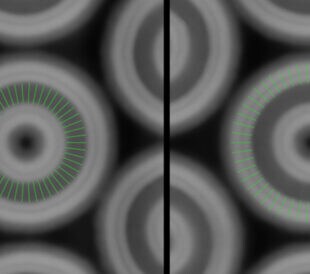
What are the key differences between TEM and STEM modes?
TEM mode:
- Uses a focused beam on the sample
- Captures transmitted electrons in a single snapshot
- Employs high-speed, high-resolution cameras
- Offers faster, simpler operation

Fig 2: Schematic illustration of TEM mode operation.
STEM mode:
- Utilizes electromagnetic scan coils
- Scans a focused beam across the sample
- Multiple detector configurations available
- Provides flexible, high-contrast imaging

Fig 3: Schematic illustration of STEM mode operation.
How has automation enhanced TEM analysis?
Modern semiconductor TEM systems feature significant automation improvements:
- Simplified parameter selection
- Automated alignment and calibration
- Reduced data distortion risk
- Atomic-scale image calibration
- Streamlined operation for various sample types
Why is TEM critical for semiconductor manufacturing?
TEM serves as the primary source for reference data in semiconductor design and fabrication due to:
- Increased 3D device complexity
- Shrinking critical dimensions
- EUV lithography requirements
- Need for atomic interface analysis
- Strain and magnetic field measurements
What are the key applications and the industry impact?
Leading semiconductor manufacturers now generate tens of thousands of TEM datasets monthly for:
- Process variation analysis
- Wafer fab tool calibration
- Defect mechanism investigation
- Quality control

Fig 4: Graph showing growth trend in semiconductor TEM analysis usage.
Summary
- TEM technology provides atomic-level imaging and analysis capabilities
- Dual-mode operation (TEM/STEM) offers flexible analysis options
- Automation advances have simplified operation and improved reliability
- Critical role in semiconductor manufacturing quality control
- Essential for next-generation device development

Enhancing High-Volume DRAM Manufacturing with Automated TEM Metrology and Characterization
Dynamic random-access memory (DRAM) plays a crucial role in ... Dr. Zhenxin Zhong
Read More
Faster time to data in the fab with multi-ion species plasma FIB
This quarter, I am excited to share the news about a newly r...
Read MoreHigh-Quality TEM Lamella Preparation: Critical Factors and Best Practices
Introduction: The quality of transmission electron microscop... Abhi Barve
Read More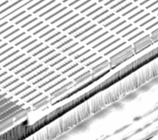
Removing Large Volumes of Material Fast with FIB-SEMs
Focused ion beam scanning electron microscopes (FIB-SEMs) ar...
Read More
Leave a Reply