Search

Talos F200E (S)透射电镜 用于快速半导体分析
Thermo Scientific Talos F200E (S)TEM(扫描透射电子显微镜)提供高分辨率的 STEM 与 TEM 成像,图像失真极小,并结合高通量的能量色散 X 射线能谱(EDS)功能,专为广泛的半导体缺陷分析与研究应用而设计。
支持快速的工艺开发和产量提升对半导体分析实验室构成重大挑战,因为它们必须对各种材料和器件提供可重复的、高分辨率表征。Talos F200E (S)TEM 专为这些实验室设计,可实现更快的 EDS 分析、降低 TEM 图像畸变,并通过 Thermo Scientific Velox软件的统一功能简化操作。 速度和可重复性方面的提升使 The Talos F200E (S)TEM 成为器件分析、缺陷表征与产量支持的理想选择。
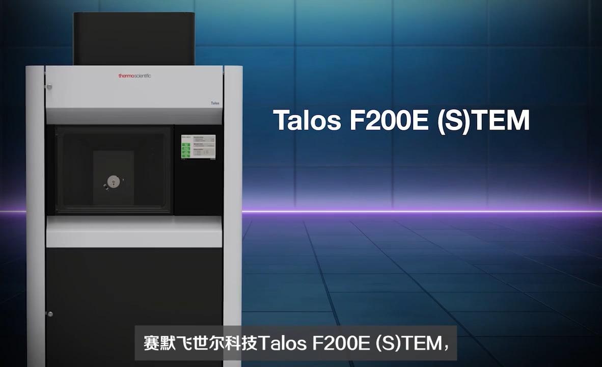
Talos F200E(S)TEM — 仪器特性


Frequently asked questions
The Thermo Scientific Talos F200E (S)TEM is designed for semiconductor laboratories that require efficient, high-resolution TEM imaging and quantitative analysis. It is well suited for semiconductor laboratories that support the characterization of power devices, memory, display technologies, advanced packaging, and other leading semiconductor structures.
The Thermo Scientific Talos F200E (S)TEM supports a wide range of semiconductor applications, including failure analysis, metrology, defect characterization, yield improvement, process development, and tomography for 3D compositional analysis. It is designed to enable fast, precise, and quantitative characterization of semiconductor devices in multiple dimensions.
The Thermo Scientific Talos F200E (S)TEM is designed to support the characterization of power and memory devices, display technologies, advanced packaging, and a wide range of other semiconductor structures that require high-resolution imaging and elemental analysis.
The Thermo Scientific Talos F200E (S)TEM offers high-resolution TEM and STEM imaging with simultaneous multi-signal detection. With the high-brightness X-CFEG, the instrument has an STEM resolution ≤0.14 nm, a TEM information limit ≤0.11 nm, and a TEM line resolution of ≤0.10 nm. These specifications support high-resolution imaging for advanced semiconductor characterization. The Talos F200E (S)TEM is also capable of integrated differential phase contrast (iDPC) imaging, high-angle annular dark field (HAADF) imaging, and contrast-optimized STEM imaging, which offer complimentary structural and compositional information.
The Thermo Scientific Talos F200E (S)TEM improves measurement reliability by combining optimized electron optics with a low-distortion camera and a stable instrument platform. These features help produce consistent, repeatable measurements across semiconductor devices.
The Thermo Scientific Talos F200E (S)TEM is capable of three-dimensional volume analysis using a combination of STEM imaging and EDS tomography, supporting the structural and compositional characterization of 3D semiconductor devices.
The Thermo Scientific Talos F200E (S)TEM improves productivity by combining automated alignment, STEM focus, and stigmation, with fast mode switching, drift-corrected frame integration, and live image rotation through synchronized stage movement. These features help you collect more high-quality data while reducing manual intervention.
Yes, the Thermo Scientific Talos F200E (S)TEM supports remote system monitoring as well as the performance of basic operations through an intranet or internet connection.
The Thermo Scientific Talos F200E (S)TEM simplifies routine operation through a number of features including the Align Genie for automated alignments, AutoSTEM for autofocus and autostigmation, and the SmartCam digital search-and-view camera for sample navigation. These features help the Talos F200E (S)TEM reduce setup time and improve reproducibility between users.
仅供研究使用。不得用于诊断用途。