Search

Aberration-corrected (S)TEM for high resolution and analytical power
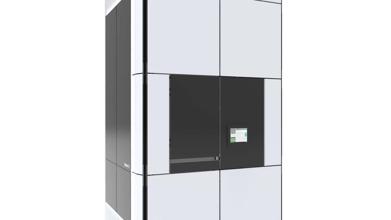
The Thermo Scientific Spectra 300 Scanning Transmission Electron Microscope ((S)TEM) is a high-end aberration-corrected TEM platform engineered for maximum resolution, sensitivity, and analytical depth at the atomic scale. Designed for advanced research in nanotechnology, semiconductors, and quantum materials, the Spectra 300 (S)TEM delivers outstanding performance through cutting-edge electron optics, enhanced stability, and fully integrated spectroscopy solutions. With optimized workflows, high-speed data acquisition, and precise control of imaging conditions, it helps researchers confidently extract deeper insights from complex materials.
Key features of Spectra 300 (S)TEM
Exceptional resolution
Sub-angstrom imaging for atomic-scale visualization.
Advanced electron optics
Aberration correction and monochromation deliver outstanding image and spectroscopy quality.
Deep analytical capability
High-sensitivity EDS and EELS provide comprehensive chemical and electronic structure analysis.
Maximum stability
Designed for ultra-high-resolution performance with advanced environmental control.
High-end research support
Tailored for next-generation materials, quantum materials, and nanotechnology.
Advanced detectors
State-of-the-art detectors provide comprehensive elemental analysis and high-sensitivity imaging.
User-friendly interface
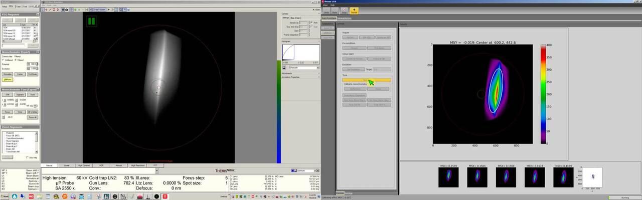
Thermo Scientific Velox Software provides an intuitive interface and automated functions.
Robust design
Acoustic enclosure minimizes outside interference. On-system display shows system status and aids sample insertion.
Innovative technology
Stay ahead of the curve with cutting-edge technology that pushes the boundaries of what’s possible in electron microscopy.
Enhanced productivity
Automated alignments and corrector tuning to help you concentrate on experiments rather than on instrument adjustments.
Comprehensive support
Backed by Thermo Fisher Scientific’s global network of experts and dedicated customer service.
Spectra 300 (S)TEM specifications
| Image corrector |
|
Probe corrector |
|
| Uncorrected |
|
X-FEG/monochromator double corrected (probe+image corrector) |
|
X-CFEG double-corrected (probe+image correction) |
|
| Source |
|
Advanced (S)TEM technologies for high-resolution materials characterization
High-energy-resolution sources available on the Spectra 300 (S)TEM
The Spectra 300 (S)TEM lets you choose between high-energy-resolution X-FEG/Mono or ultra-high-energy-resolution X-FEG/UltiMono. With OptiMono and OptiMono+, maximum performance is just a single click away. Advanced hardware and intelligent automation work together to deliver clarity and precision without the complexity. See the difference in the video.
High-resolution STEM imaging performance for all accelerating voltages
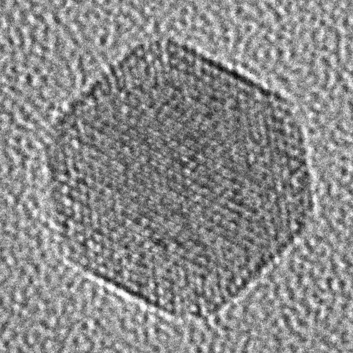
With fifth-order aberration correction, high stability, and the S-TWIN Wide-Gap Pole Piece, the Spectra 300 (S)TEM achieves 50 pm at 300 kV, 96 pm at 60 kV, and 125 pm at 30 kV. With X-CFEG, probe currents reach 100 pA for the system’s ultimate clarity and analytical power. For a full list of specifications, please refer to the Spectra 300 (S)TEM datasheet.
Ultra-high-brightness cold field emission gun (X-CFEG)
The Spectra 300 (S)TEM with X-CFEG achieves sub-angstrom resolution below 0.8 Å while driving probe currents beyond 1000 pA. Its extreme brightness and ultra-low energy spread unlock faster acquisition, higher throughput, and outstanding clarity in every image.
High sensitivity with the Pather STEM detection system
The Panther STEM Detection System takes imaging on the Spectra (S)TEM to an entirely new level. Its advanced architecture and 16-segment solid-state detectors deliver breakthrough contrast capabilities with sensitivity so high it can measure single electrons.
 With the Panther STEM System, SrTiO₃ [001] HAADF images remain sharp even below 1 pA. Exceptional signal-to-noise enables OptiSTEM+ to auto-correct aberrations for outstanding clarity.
4D STEM imaging capabilities across 30 to 300 kV
The Spectra 300 (S)TEM offers excellent 4D STEM with the electron microscope pixel array detector (EMPAD). Operating from 30 to 300 kV, EMPAD combines one-million-to-one dynamic range, single electron sensitivity, and 1100 fps speed on a 128 × 128 array. From the brightest central beam to the faintest diffraction, it captures every detail and supports applications like ptychography.
 The EMPAD detector can be used for a wide variety of applications. On the left, it is used to extend spatial resolution (0.39 Å) beyond the aperture-limited resolution at low accelerating voltages (80 kV) in a bi-layer of the 2D material MoS2 (Jiang, Y. et al. Nature 559, 343–349, 2018). On the right, it is used to independently image dark field reflections, revealing the complex microstructure of the precipitates in a superalloy. Sample courtesy Professor G. Burke, University of Manchester.
EDS and EELS in STEM analytics with Spectra 300 (S)TEM
The Spectra 300 (S)TEM delivers spectroscopic flexibility with fast, high signal-to-noise elemental mapping and ultra-high-resolution EELS that probes oxidation states and surface phonons. It can be equipped with your choice of three electron sources, two EDS geometries, and a full suite of Gatan Continuum spectrometers and filters to adapt to your research needs.
 DyScO3 specimen investigated with the powerful combination of ultra-high-brightness X-CFEG, S-CORR, and the large solid angle (1.76 Sr) of the Dual-X Detectors, resulting in high signal-to-noise ratio, atomic resolution (up to 90 pm), and unfiltered EDX maps. Sample courtesy Professor L.F. Kourkoutis, Cornell University.
In situ (S)TEM capabilities of the Spectra 300 (S)TEM
The Spectra 300 (S)TEM makes in situ experiments simple with its all-in-one S-TWIN Wide-Gap Pole Piece. Combined with Thermo Scientific NanoEx Holders, it enables MEMS-based heating for atomic imaging at elevated temperatures with ease.
Gold nanoparticles heated to 700°C were recorded in real time at over 30 fps and full-frame 4k resolution on a Thermo Scientific Ceta Camera, quickly and clearly capturing dynamic molecular behavior.
On the left is a high frame rate movie of gold nano-islands at high temperature, collected on a Ceta Camera with speed enhancement. On the right, the 4k x 4k sensor allows digital zoom while maintaining high resolution in the field of interest.

Spectra 300 resources
Watch the webinar and explore the documents below to learn more about how the Spectra 300 (S)TEM can support your materials science research.
TEM webinar")
Spectra 300 (S)TEM documentation
TEM datasheet thumbnail")
For Research Use Only. Not for use in diagnostic procedures.