Search

Fully integrated atomic-resolution (S)TEM imaging and spectroscopy
The Thermo Scientific Spectra Ultra Scanning Transmission Electron Microscope ((S)TEM) delivers the highest-resolution imaging and spectroscopy of the Spectra (S)TEM family. By uniting state-of-art hardware and intelligent software in one system, it delivers atomic-level resolution, advanced spectroscopy, and automated workflows that make outstanding performance routine.
Key features of the Spectra Ultra (S)TEM
Constant-power objective lens
Atomic-scale clarity across all high tensions.
Integrated Ultra-X Detectors and Thermo Scientific Velox Software
Fast, sensitive, and intuitive analysis.
Guided workflows and automation
Easy operation with automated alignments, corrector tuning, and intuitive workflows turn complex experiments into routine tasks.
Versatility for a variety of fields
From clean energy and quantum research to metals, alloys, semiconductors, and catalysts.
Innovative technology
High stability and vibration isolation, acoustic shielding, and built-in monitoring.
Global expertise
Backed by Thermo Fisher Scientific’s worldwide network of specialists and dedicated service.
Spectra Ultra (S)TEM specifications
Uncorrected |
|
| Probe corrected |
|
| Probe+Image corrected X-FEG/Mono |
|
| Probe+Image corrected X-FEG/UltiMono |
|
Probe+Image corrected X-CFEG |
|
| Source |
|
Advanced STEM imaging, EDX analysis, and automation features
Fast, optimized results from more materials
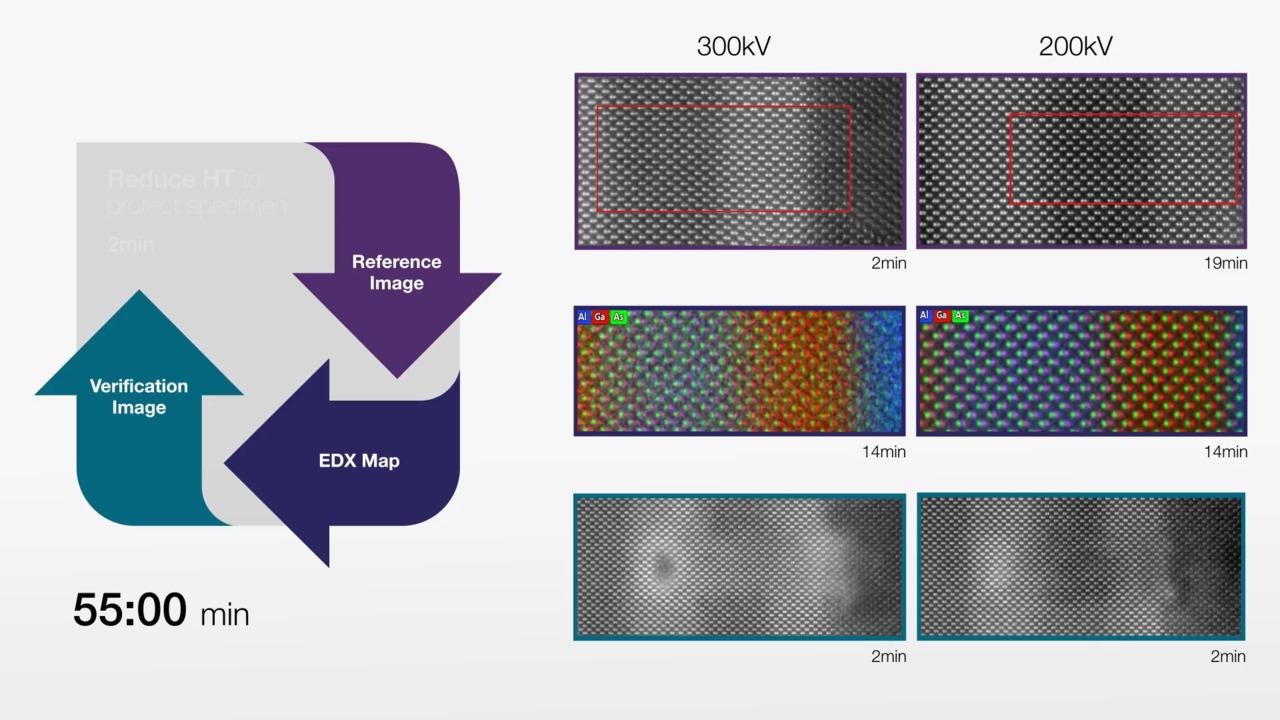
The Spectra Ultra (S)TEM uses a constant-power objective lens to maintain stability from 30 kV to 300 kV, reducing stabilization time from hours to less than five minutes. Switching voltages is easy, keeping the focus on results. Imaging at 300 kV captures atomic-resolution detail, while imaging at lower voltages delivers optimized STEM EDX mapping with higher X-ray yields, reduced damage, and high-sensitivity EDX detection with the Ultra-X Detector.
Low-dose STEM EDX for characterizing more materials
The Spectra Ultra (S)TEM introduces the Ultra-X Detector, our most sensitive EDX detector. With a solid angle above 4.45 sr, it unlocks new possibilities in STEM EDX. Even with an analytical double tilt holder, performance remains above 4.04 sr.
 Normalized count-rates as function of tilt angle for the Super-X, Dual-X, and Ultra-X Detectors. Data was recorded at 200 kV with optimized specimen holders for each detector configuration. Zaluzec, et al. Submitted to Microscopy and Microanalysis, 2021.
 A quantitative comparison is shown between Super-X, Dual-X, and Ultra-X on a DyScO3 specimen. The improvements in the signal-to-noise ratio are clearly seen. Specimen courtesy of L.F. Kourkoutis, Cornell University.
The Ultra-X Detector delivers spectrum imaging with outstanding sensitivity. On a DyScO₃ specimen, it achieves an excellent signal-to-noise ratio and reveals the oxygen lattice, details not visible with Super-X or Dual-X Detectors.
Additionally, the high sensitivity of the Ultra-X Detector allows it to obtain the same level of chemical information with a fraction of the electron dose that would be required for other EDX detectors. This opens possibilities for STEM EDX analysis of more beam-sensitive specimens and faster mapping for more stable specimens.
 Comparable line profiles extracted from the spectrum images demonstrate that a similar signal-to-noise ratio can be obtained with Ultra-X Detector with only a fraction of the electron dose needed for the Super-X Detector. Specimen courtesy of L.F. Kourkoutis, Cornell University.
High-resolution STEM imaging performance across 30 to 300 kV accelerating voltages
The Spectra Ultra (S)TEM features the new S-TWIN Prime Pole Piece, combining ultra-high spatial resolution with a wide gap for large tilt angles and bulky in situ holders. It achieves 50 pm at 300 kV and 96 pm at 60 kV while supporting high solid-angle EDX without sacrificing resolution. With enhanced mechanical stability and the latest S-CORR probe corrector, the S-TWIN Prime Pole Piece delivers high resolution and high probe current performance, matching the advanced specifications of the Spectra 300 TEM.
 DyScO3 specimen investigated with the powerful combination of ultra-high brightness X-CFEG, S-CORR and the large solid angle (1.76 Sr) of the Dual-X Detectors, resulting in high signal-to-noise ratio, atomic resolution (up to 90 pm), and unfiltered EDX maps. Sample courtesy Professor L.F. Kourkoutis, Cornell University.
High-energy resolution and high-brightness sources
The Spectra Ultra (S)TEM offers a choice of the X-FEG/Mono source or the ultra-high-resolution X-FEG/UltiMono source. Both OptiMono and OptiMono+ deliver peak energy resolution with one-click automatic tuning.
The X-FEG/Mono source reaches 0.2 eV, while the X-FEG/UltiMono source achieves below 25 meV. Both operate from 30 to 300 kV and can run in standard mode for maximum brightness, supporting STEM-EDS mapping, ultra-high-resolution STEM, and high-current TEM imaging without
High-sensitivity STEM detection system for single-electron imaging
STEM imaging on the Spectra (S)TEM is redefined with the Panther Detection System. Its new architecture and 16-segment solid-state detectors unlock advanced imaging modes with the sensitivity to detect single electrons.
 Comparison of SrTiO₃ [001] HAADF images taken with the Panther STEM Detection System with 3 pA, 1.3 pA, and <1 pA of probe current. Even with probe currents <1 pA, the signal-to-noise ratio in the image allows automation routines like OptiSTEM+ to correct first and second order aberrations in the probe forming optics, delivering sharp images.
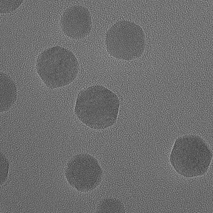
Advanced STEM imaging and 4D STEM data acquisition capabilities
The Spectra Ultra (S)TEM can be configured with an electron microscope pixel array detector (EMPAD) or a Thermo Scientific Ceta Camera with speed enhancement to collect 4D STEM data sets.
The EMPAD is capable of 30 to 300 kV imaging and provides a high dynamic range (1:1,000,000 e- between pixels), high signal-to-noise ratio (1/140 e-), and high speed (1,100 frames per second) on a 128 x 128 pixel array, which makes it an outstanding choice for 4D STEM applications where the details of the central and diffracted beams need to be analyzed simultaneously, as in the ptychography image shown here.
The Ceta Camera with speed enhancement offers an alternative for 4D STEM applications where more pixels are required and when EDS analysis needs to be combined with each point in the STEM scan. This solution provides higher resolution diffraction patterns (up to 512 x 512-pixel resolution), suited for applications such as strain measurement.
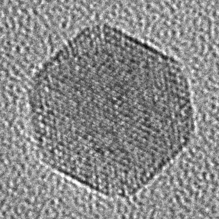
 The EMPAD detector can be used for a wide variety of applications. On the left, it is used to extend spatial resolution (0.39 Å) beyond the aperture-limited resolution at low accelerating voltages (80 kV) in a bi-layer of the 2D material MoS₂ ( Jiang, Y. et al. Nature 559, 343–349, 2018). On the right, it is used to independently image dark field reflections, revealing the complex microstructure of the precipitates in a superalloy. Sample courtesy Professor G. Burke, University of Manchester.
In situ capabilities of the Spectra Ultra (S)TEM
The Spectra Ultra (S)TEM, equipped with the all-in-one S-TWIN Prime Pole Piece, supports a broad range of in situ experiments. Its integration with Thermo Scientific NanoEx Holders enables MEMS-based heating for atomic-scale imaging at elevated temperatures. In the example shown here, gold nanoparticles are heated to 700°C and recorded in real time at over 30 fps in full 4k × 4k resolution using a Ceta Camera with speed enhancement, capturing dynamic molecular behavior with exceptional spatial and temporal precision.
On the left is a high frame rate movie of gold nano-islands at high temperature, collected on a Ceta Camera with speed enhancement. On the right, the 4k x 4k sensor allows digital zoom while maintaining high resolution in the field of interest.
Spectra Ultra (S)TEM resources for materials analysis
Watch the webinar and explore the documents below to learn more about how the Spectra Ultra (S)TEM can support your materials science research.
TEM and EDX")
Spectra Ultra (S)TEM documentation
TEM for Materials Science datasheet")
TEM for Semiconductors datasheet")
For Research Use Only. Not for use in diagnostic procedures.