Helios MX1 PFIB-SEM overview

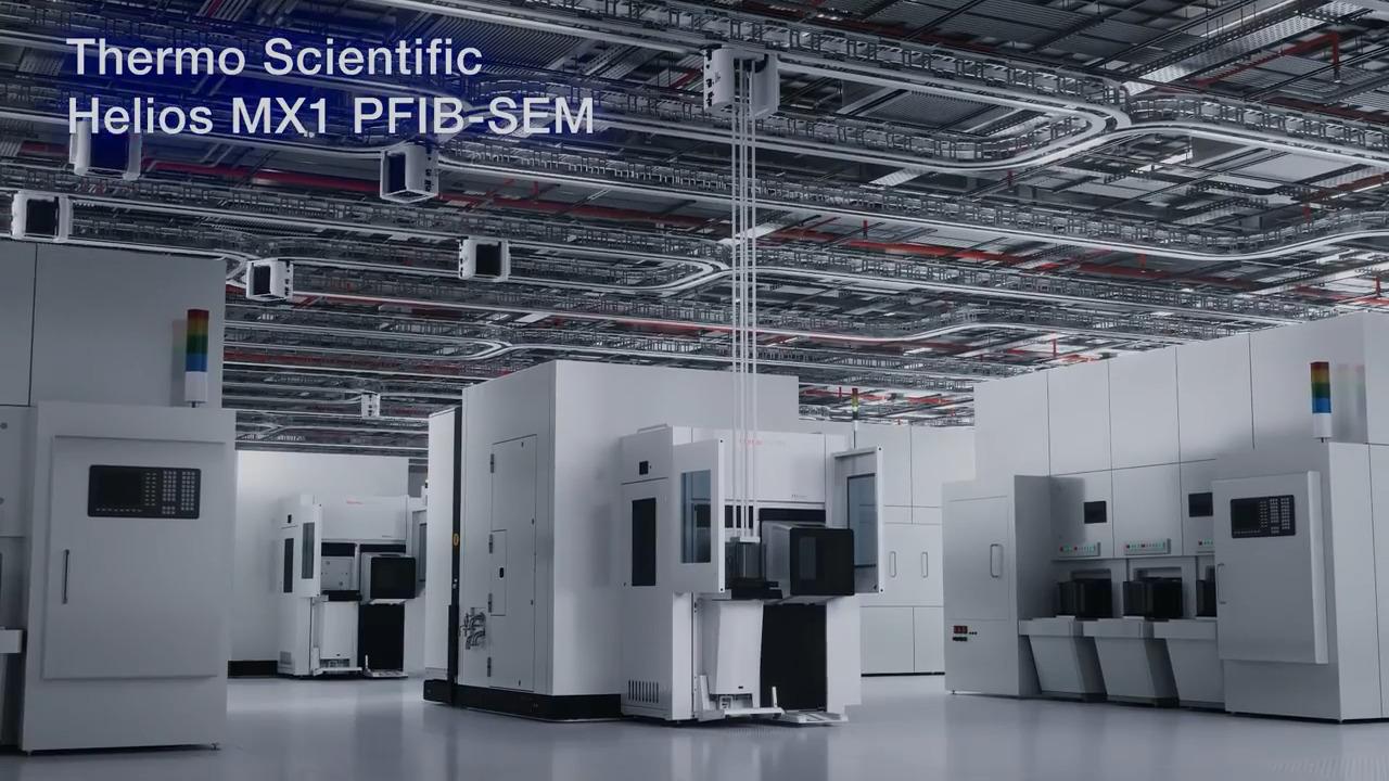
Introducing the Thermo Scientific Helios MX1 PFIB-SEM, designed to accelerate time-to-data for semiconductor yield ramp and fab process control. This automated system enables rapid, high-throughput analysis of full 300 mm wafers, with fab host connectivity that supports integration into fab or lab environments. With new multi-ion species plasma FIB technology, ultra-high-resolution SEM imaging, and powerful automation, the Helios MX1 PFIB-SEM facilitates fast, accurate, through volume critical dimension profiles (3D metrology) and defect analysis of buried structures beyond the reach of traditional fab systems. Take control of your process, increase yield, and own your data with a tool built for precision, speed, and reliability.

Helios MX1 PFIB-SEM instrument features

Built for the fab and the lab

With in-line 300 mm wafer loading and fab host connectivity, the Helios MX1 PFIB-SEM can be placed in the fab or the lab.

Multi-ion-species plasma FIB

The Helios MX1 PFIB-SEM features switchable argon and xenon ion sources, providing excellent flexibility and enabling optimized milling for specific metrology and defect applications.

High-throughput volume removal

Revealing buried structures for large-volume applications can be achieved with beam currents up to 6 μA using the argon plasma source, enabling a 20x throughput improvement compared to gallium milling.

Precise 3D metrology

Obtain through volume critical dimension profiles with ultra-high-resolution SEM imaging and innovative metrology solutions that help ensure precision, stability, and throughput, without compromise.

Automated 3D reconstruction

Integrated workflows create 3D volumes of semiconductor devices. Easily visualize device interfaces and buried defects with the 3D viewer.

Virtual slice metrology

Access device profiles and critical dimension trends through automated virtual-slice extraction from reconstructed 3D volumes.

For Research Use Only. Not for use in diagnostic procedures.