Resources for semiconductor analysis with the Helios MX1 PFIB-SEM

Welcome to our dedicated resource page for the latest insights into fab process control with the Thermo Scientific Helios MX1 PFIB-SEM. Whether you're an experienced professional or new to the field, this is your go-to destination for up-to-date information on emerging trends and technologies. Our resources are designed to help you navigate the complex world of metrology and defect analysis with ease, offering in-depth technical discussions and practical guidance. Take a moment to explore and discover the valuable content we offer.


Frequently asked questions about the Helios MX1 PFIB-SEM

  • What is the Helios MX1 PFIB-SEM?
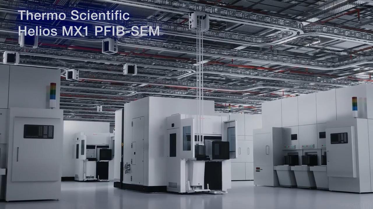
    The Thermo Scientific Helios MX1 PFIB-SEM is a plasma focused ion beam scanning electron microscope designed to meet the evolving challenges of semiconductor fabs, bringing 3D SEM metrology and defect analysis in-line. It accelerates time-to-data for semiconductor manufacturers, helping to improve yield ramp and maintain in-line process control for advanced 3D architectures and buried structures.

  • How does the multi-ion-species plasma FIB of the Helios MX1 system support SEM metrology of semiconductor devices?
    Newly available with the Helios MX1 PFIB-SEM is a multi-species plasma ion source, which can quickly swap between argon and xenon gas species for FIB milling. This allows you to alternate between optimized high-volume material removal and precision milling, supporting high-quality diagonal mill, delayering, and cross sectioning.

  • What automation features support in-line metrology with the Helios MX1 PFIB-SEM?
    The Helios MX1 PFIB-SEM features new Metrology Studio Software, a streamlined user interface for recipe development that includes SMART targeted activities built for common measurement types. Running on a GPU-enabled SDP server, Metrology Software accelerates time to recipe and overall process throughput.

    Additionally, a single SECS/GEM connection enables factory automation and factory host communication. System availability and reliability are supported by an in-chamber, fixed sample calibration standard, which is used for system monitoring and calibration during wafer load cycles. This leads to reduced downtime and SPC-monitored validation of system performance.

  • What semiconductor failure analysis and metrology applications are supported by the Helios MX1 PFIB-SEM?
    The Helios MX1 PFIB-SEM supports wafer-level defect analysis through a number of critical analytical techniques.

    Diagonal milling with the high-throughput argon PFIB enables rapid and precise nanometer-scale through-stack measurement of critical device structures, which were inaccessible to traditional in-line metrology. Engineers can quickly assess etching quality, bowing, twisting, and CD variation, improving fab process control and performance optimization.

    Large-area planar delayering, using a combination of proprietary gas chemistry and xenon PFIB, supports high-resolution SEM metrology directly in the fab, accelerating feedback and high-volume data collection. With automated end-pointing, material is removed and tracked, allowing precise layer by layer mill control that captures thousands of through-stack CD measurements per memory cell.

    High-throughput cross-sectioning is made possible by argon PFIB milling, quickly exposing defects for high-resolution SEM imaging. The addition of integrated metrology software offers automated measurements, helping to deliver critical metrology data directly within the fab.

Helios MX1 PFIB-SEM videos


Datasheets

Helios MX1 PFIB-SEM datasheet

The Helios MX1 PFIB-SEM is designed for acquiring rapid through volume critical dimension profiles and defect analysis of 300 mm wafers. Featuring a multi-ion source plasma FIB, ultra-high-resolution SEM, and powerful automation, it is well-suited for memory, logic, and advanced packaging applications.


Helios MX1 PFIB-SEM publications

Blog: Helios MX1 PFIB-SEM: Addressing fab process control needs with plasma FIB technology

Read the viewpoint from our VP/GM Semiconductor on how Helios MX1 PFIB-SEM plasma FIB technology can address unmet needs in semiconductor fabs.

Blog: Advanced Semiconductor Packaging: Bringing Stacked Chips Together

Learn more about the challenges in advanced packaging and how our electrical and physical failure analysis systems support fault isolation and defect characterization. 

For Research Use Only. Not for use in diagnostic procedures.