Search

Direct electron detector for 4D STEM
Advanced STEM experiments often require quantitative diffraction information from every probe position, not just an image. The Thermo Scientific EMPAD G2 Detector for 4D STEM supports strain mapping, crystal orientation analysis, electromagnetic field mapping, and ptychographic phase reconstruction in a unified acquisition workflow.
The EMPAD G2 Detector is available on Thermo Scientific transmission electron microscopes for materials science and semiconductor analysis and it natively integrates with Thermo Scientific Velox Software.
The EMPAD G2 Detector is available in two versions: EMPAD G2 Single with 128 × 128 pixels and EMPAD G2 Quad with 256 × 256 pixels.

Applications for quantitative 4D STEM data
The EMPAD G2 Detector supports materials science and semiconductor applications where researchers need to measure structural, electromagnetic, or crystallographic information from diffraction data. The examples below show how high-DQE, high-dynamic-range detection can support magnetic imaging, semiconductor metrology, orientation mapping, and strain mapping.
Magnetic imaging with Lorentz electron ptychography
When nanoscale magnetic textures are difficult to resolve, Lorentz electron ptychography can help visualize magnetic structure with high resolution and sensitivity.
Using the EMPAD G2 Detector, researchers resolved the internal magnetic structure of FeGe skyrmions, including features at skyrmion cores, boundaries, and dislocations.
High DQE, high dynamic range, and high current handling help preserve quantitative diffraction information for magnetic field measurement and ptychographic reconstruction.

Color-coded magnetic vector map with directional arrows and 50 nm scale bar.
Image courtesy of Chen Z., Turgut E., Jiang Y., Nguyen K.X., Stolt M.J., Jin S., et al., Nat. Nanotechnol. 2022, 17, 1165–70.
3D atomic-scale metrology for next-generation semiconductor devices
Advanced semiconductor devices contain buried structures that need metrology before electrical testing and defect analysis. Multislice electron ptychography with the EMPAD G2 Detector enables quantitative 3D imaging of buried gate-all-around transistor structures from a single 4D STEM dataset.
Atomic-scale strain, interface roughness, buried defects, and structural variations can be measured together to support process-development feedback for next-generation devices.
Ruthenium via orientation mapping
In thin front-end-of-line vias, grain structure can affect product reliability when heavier metals such as tungsten or ruthenium are used to help reduce electron-migration damage.
Orientation mapping with the EMPAD G2 Detector can be used to evaluate ruthenium via grain size and correlate the structure with growth conditions.
 Color-coded orientation map of a ruthenium via.
Gate-all-around forksheet imaging
One approach to implementing complementary transistors with gate-all-around technology is the forksheet structure.
In this view, the SiGe layers have been partially etched, leaving the silicon channel protruding outward. High-aspect-ratio standing pairs can develop strain or bending, which can be evaluated with high-resolution strain mapping.
 Color-coded strain map of a gate-all-around (GAA) forksheet structure.
Key features of the EMPAD G2 Detector
The EMPAD G2 Detector is designed for quantitative 4D STEM workflows that require a high signal-to-noise ratio, broad dynamic range, high current handling, and integration with Thermo Scientific TEM data acquisition and analysis software. The features below explain how detector performance, voltage range, and integration with Velox Software support materials science and semiconductor applications.


4D STEM applications for structure and field mapping
4D STEM collects a diffraction pattern at each probe position, allowing you to reconstruct phase, map fields, measure strain, and quantify orientation from diffraction data. The EMPAD G2 Detector supports these applications for materials science and semiconductor research when quantitative diffraction information is needed.


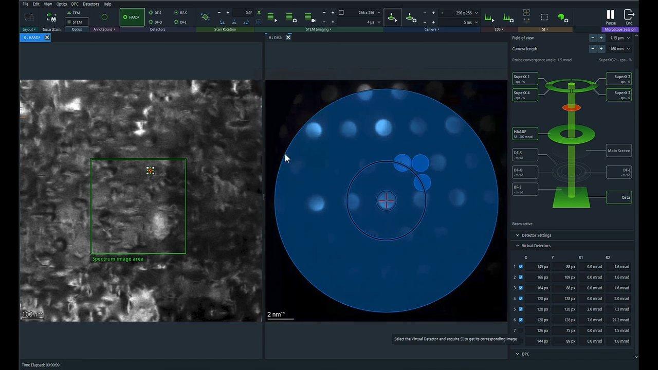
Integrated 4D STEM workflow with Velox Software
4D STEM workflows are easier to reproduce when acquisition, live visualization, metadata, and offline processing are connected. The EMPAD G2 Detector brings 4D STEM into the native Velox Software environment, allowing you to acquire 4D STEM, STEM imaging, and EDS data, visualize diffraction patterns in real time with virtual detectors, and move from acquisition to quantitative analysis with synchronized metadata and integrated processing.
EMPAD G2 Detector specifications
Use the specifications below to evaluate the EMPAD G2 Detector for quantitative 4D STEM workflows, including sensor format, dynamic range, current handling, speed, voltage range, software compatibility, and system requirements.
| Sensor dimensions | Active area |
19.2 x 19.2 mm or 38.4 x 38.4 mm |
|---|---|---|
| Pixels | Single 128 x 128 or Quad 256 × 256 | |
| Pixel size | 150 x150 μm | |
| Active thickness | 500 μm | |
| Performance | DQE(0): |
|
| Dynamic range | 107:1 across all exposure times | |
| Max current/pixel |
|
|
SNR |
|
|
| High-tension range | 30 to 300 keV | |
| Maximum speed | 10,000 fps at full well capacity | |
| Storage capacity | Internal storage: 6 TB (standard) | |
| Additional storage: 24 TB (optional) | ||
| Control and imaging software |
|
|
| System requirements |
|
|
| Retrofit | For retrofits on your tool, contact the sales and service organization in your region. | |
Ask the inventors
Resources

Frequently asked questions about the EMPAD G2 Detector
The EMPAD G2 Detector is used to acquire diffraction information from every probe position in a 4D STEM experiment, supporting applications such as ptychography, strain mapping, orientation mapping, magnetic imaging, and semiconductor metrology.
Velox Software integration allows researchers to acquire 4D STEM data alongside STEM imaging and EDS data, visualize diffraction patterns in real time with virtual detectors, and process 4D STEM datasets within a connected workflow.
The EMPAD G2 Detector supports materials science and semiconductor applications, including atomic-resolution ptychography, differential phase contrast field mapping, crystal orientation mapping, strain mapping, magnetic imaging, and 3D semiconductor metrology.
The EMPAD G2 Single Detector has 128 × 128 pixels and the EMPAD G2 Quad has 256 × 256 pixels.
For Research Use Only. Not for use in diagnostic procedures.