Search

Automated, high-efficiency (S)TEM for routine and advanced materials analysis
The Thermo Scientific Spectra 200 Scanning Transmission Electron Microscope (STEM) is an aberration-corrected TEM platform designed to deliver high-resolution imaging and analytical performance across a broad range of materials science and semiconductor applications. Combining atomic-scale resolution with flexible configuration options, the Spectra 200 (S)TEM enables detailed structural and chemical characterization for research in energy materials, catalysts, and metals. Integrated advanced detectors and intuitive Thermo Scientific Velox Software streamline data acquisition and analysis, while robust system stability and automated alignments support consistent, high-quality results and efficient daily operation.
Key features of Spectra 200 (S)TEM
Atomic-scale resolution
High-resolution imaging with advanced electron optics for precise structural and compositional analysis.
Application versatility
Optimized for energy materials, catalysts, metals, semiconductors, and academic research environments.
Integrated analytics
Advanced EDS and STEM detectors for routine, high-quality characterization.
Ease of use
Automated alignments and Velox Software simplify workflows and reduce operator complexity.
Stable and reliable performance
Engineered for consistent results in multi-user and high-throughput labs.
Robust design
Acoustic enclosure minimizes outside interference. On-system display shows system status and aids sample insertion.
Innovative technology
Stay ahead of the curve with cutting-edge technology that pushes the boundaries of what’s possible in electron microscopy.
Enhanced productivity
Automated alignments and corrector tuning to help you concentrate on experiments rather than on instrument adjustments.
Comprehensive support
Backed by Thermo Fisher Scientific’s global network of experts and dedicated customer service.
Spectra 200 (S)TEM specifications
Probe corrector |
|
| Source |
|
| Uncorrected |
|
Analytics and detectors |
|
Available detector options |
|
Advanced Spectra 200 (S)TEM features
Ultra-high-brightness cold field emission gun (X-CFEG)
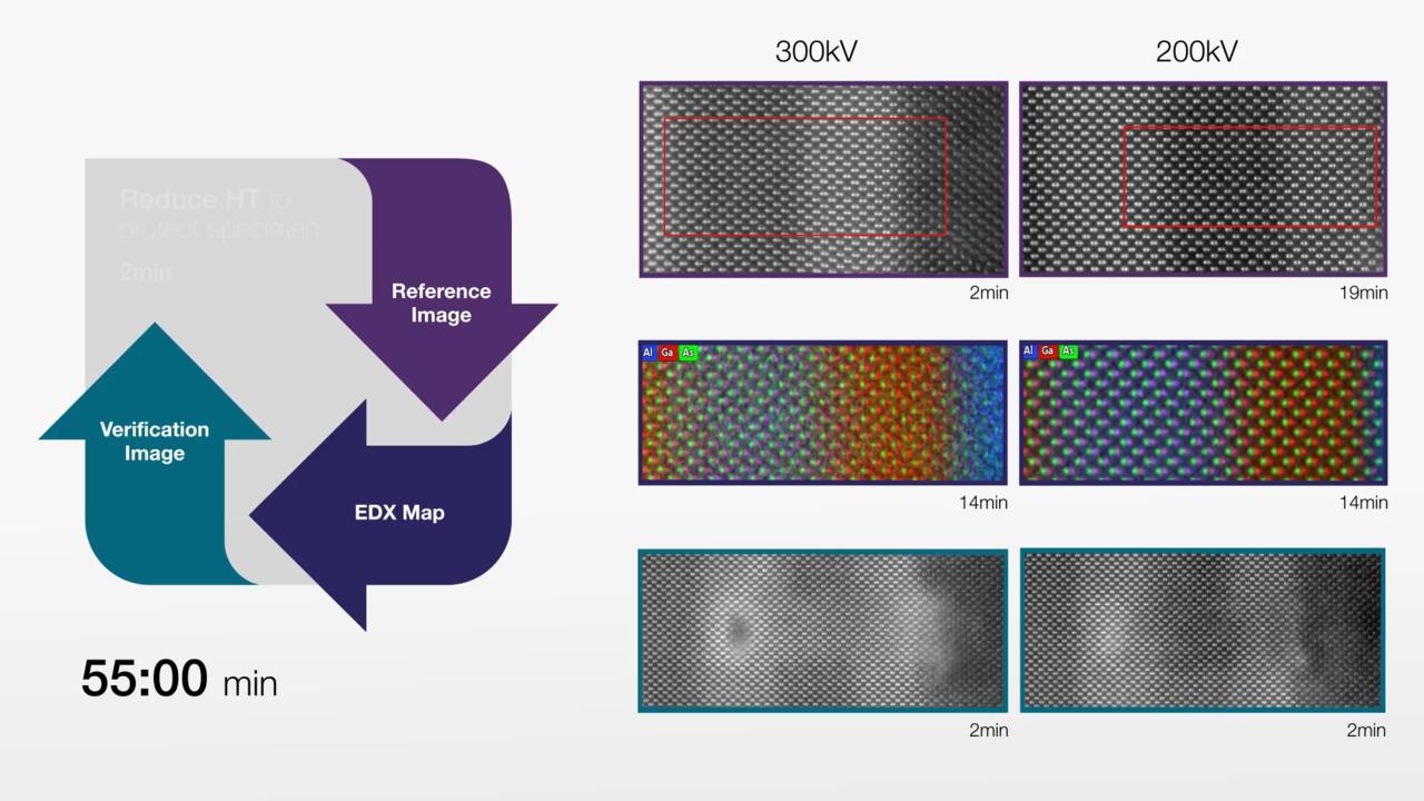
The Spectra 200 (S)TEM is equipped with an extreme-cold field emission gun (X-CFEG). The X-CFEG has extremely high brightness (>>1.0 x 10⁸ A/m2/Sr/V*) and low energy spread, and it can be operated from 30 to 200 kV. This provides high-resolution STEM imaging with high probe currents for high-throughput, fast-acquisition STEM analytics. With the powerful combination of X-CFEG and S-CORR probe aberration corrector, sub-Angstrom STEM imaging with over 1000 pA of probe current can be routinely achieved. Thanks to the inherent lower energy spread, the highest STEM resolution at lower HT’s is easy to do on this platform.
High-resolution STEM imaging performance for all accelerating voltages
The combination of enhanced mechanical stability, the latest fifth-order S-CORR probe aberration correction, and the X-CFEG gives the Spectra 200 (S)TEM high-resolution, high-contrast STEM imaging capability for all accelerating voltages. Additionally, the Spectra 200 (S)TEM retains the wide gap S-TWIN objective lens as standard from the Themis product line to provide a pole gap with “room to do more” without compromising on spatial resolution.
 Si [110] and GaN [212] taken on a Spectra 200 (S)TEM showing the specified resolution on a wide gap analytical S-TWIN Pole Piece (green circle) and achievable resolution (red circles). At 60 kV, 96 pm resolution is specified, and at 200 kV, 60 pm is specified with an achievable resolution of <48 pm.
High sensitivity with the Panther STEM detection system
STEM imaging on the Spectra 200 (S)TEM is performed with the Panther STEM Detection System. It includes a new data acquisition architecture and two new, solid-state, eight-segment ring and disk STEM detectors (16 segments in total). The new detector geometry offers access to advanced STEM imaging capability combined with great low electron dose performance.
 Comparison of SrTiO₃ [001] HAADF images taken with the Panther STEM Detection System with 3 pA, 1.3 pA, and <1 pA of probe current. Even with probe currents <1 pA, the signal-to-noise ratio in the image allows automation routines like OptiSTEM+ to correct first- and second-order aberrations in the probe forming optics, delivering sharp images.
Advanced STEM imaging capabilities
The Spectra 200 (S)TEM can be configured with an electron microscope pixel array detector (EMPAD) or a Thermo Scientific Ceta Camera with speed enhancement to collect 4D STEM data sets.
The EMPAD is capable of 30 to 300 kV imaging and provides a high dynamic range (1:1,000,000 e- between pixels), high signal-to-noise ratio (1/140 e-), and high speed (1100 frames per second) on a 128 x 128 pixel array, which makes it an optimal detector for 4D STEM applications where the details of the central and diffracted beams need to be analyzed simultaneously, as in the ptychography image shown here.
 The EMPAD can be used for a wide variety of applications. On the left, it is used to extend spatial resolution (0.39 Å) beyond the aperture-limited resolution at low accelerating voltages (80 kV) in a bi-layer of the 2D material MoS2 ( Jiang, Y. et al. Nature 559, 343–349, 2018). On the right, it is used to independently image dark field reflections, revealing the complex microstructure of the precipitates in a superalloy. Sample courtesy Professor G. Burke, University of Manchester.
New possibilities in STEM analytics with Spectra 200 (S)TEM
The Spectra 200 (S)TEM is configured to be a STEM analytics powerhouse. The extreme brightness and low energy spread of the X-CFEG, the latest generation fifth-order S-CORR probe corrector, the wide gap S-TWIN Pole Piece with a portfolio of large solid-angle, in-column, and symmetric EDS detectors, and the built-in EDX quantification engine in Velox Software makes STEM EDX on Spectra 200 (S)TEM fast, easy, and quantifiable.
 DyScO3 specimen investigated with the powerful combination of ultra-high brightness X-CFEG, S-CORR and the large solid angle (1.76 Sr) of the Dual-X Detectors, resulting in high signal-to-noise ratio, atomic resolution (up to 90 pm), and unfiltered EDX maps. Sample courtesy Professor L.F. Kourkoutis, Cornell University.
Spectra 200 (S)TEM resources
Watch the webinar and explore the documents below to learn more about how the Spectra 200 (S)TEM can support your materials science research.
TEM webinar")
Spectra 200 (S)TEM documentation
TEM for Materials Science datasheet thumbnail")
For Research Use Only. Not for use in diagnostic procedures.